
Aditya Nirmale, Yan Li, Seiichiro Izawa, Minoru Osada, Yutaka Majima*
Abstract
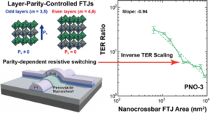
Ferroelectric tunnel junctions (FTJs) are promising for next-generation high-density non-volatile memory; however, conventional polycrystalline oxide FTJs face issues with defect-induced leakage and degraded ferroelectricity at nanometer scales. Here, we demonstrate atomically defined nanocrossbar FTJs based on single-crystalline two-dimensional (2D) Dion–Jacobson perovskite nanosheets designed to address these scaling challenges. Electrical transport measurements reveal crystallographic-parity-dependent switching behavior: odd-layered (m = 3, 5) homologs exhibit hysteretic switching consistent with ferroelectric tunnel barriers, whereas even-layered (m = 4, 6) homologs show non-switching behavior consistent with paraelectric controls. Simmons-model analysis supports direct tunneling as the dominant transport mechanism through the atomically uniform nanosheet barriers, even at the smallest junction area of 520 nm2. Notably, the tunneling electroresistance (TER) ratio increases as the junction area decreases, reaching approximately 35, consistent with the suppression of defect-induced OFF-state current inhomogeneity under nanoconfinement. These FTJs show strong non-volatile retention (extrapolated to 10 years) and reliable switching endurance (100 cycles) at room temperature. These results highlight that crystallographic layer parity and nanoconfinement-enabled defect avoidance serve as key design principles for scalable 2D ferroelectric tunnel devices and facilitate pathways toward ultra-dense post-Moore memory and neuromorphic computing architectures. This favorable scaling behavior aligns lateral miniaturization with improved memory contrast and, together with the metal-electrode nanocrossbar architecture, provides a promising basis for high-density integration if wafer-scale nanosheet assembly and reproducible interface control can be established.